Materials with potential / Growing through holes
Silicon carbide is an up-and-coming semiconductor material. In a thesis project, the qualities of the crystals and the epitaxial layers underwent precise analysis. Another project combines the advantages of crystalline thin-film solar cells with a back contact structure.
Silicon carbide (4H-SiC) is the ideal semiconductor material for power electronics. For instance, efficient power converters for electric vehicles or photovoltaic systems can be produced - as well as electronics that work at high temperatures. Until now, however, very few electron devices made of silicon carbide are on the market. The reason for this: The quality of the crystals and epitaxial layers is not yet sufficient for the demanding applications because even the slightest material defects, in form of dislocations, can lead to a malfunction of the component. Dislocations are deviations from the ideal crystal lattice structure, which may occur in different types.
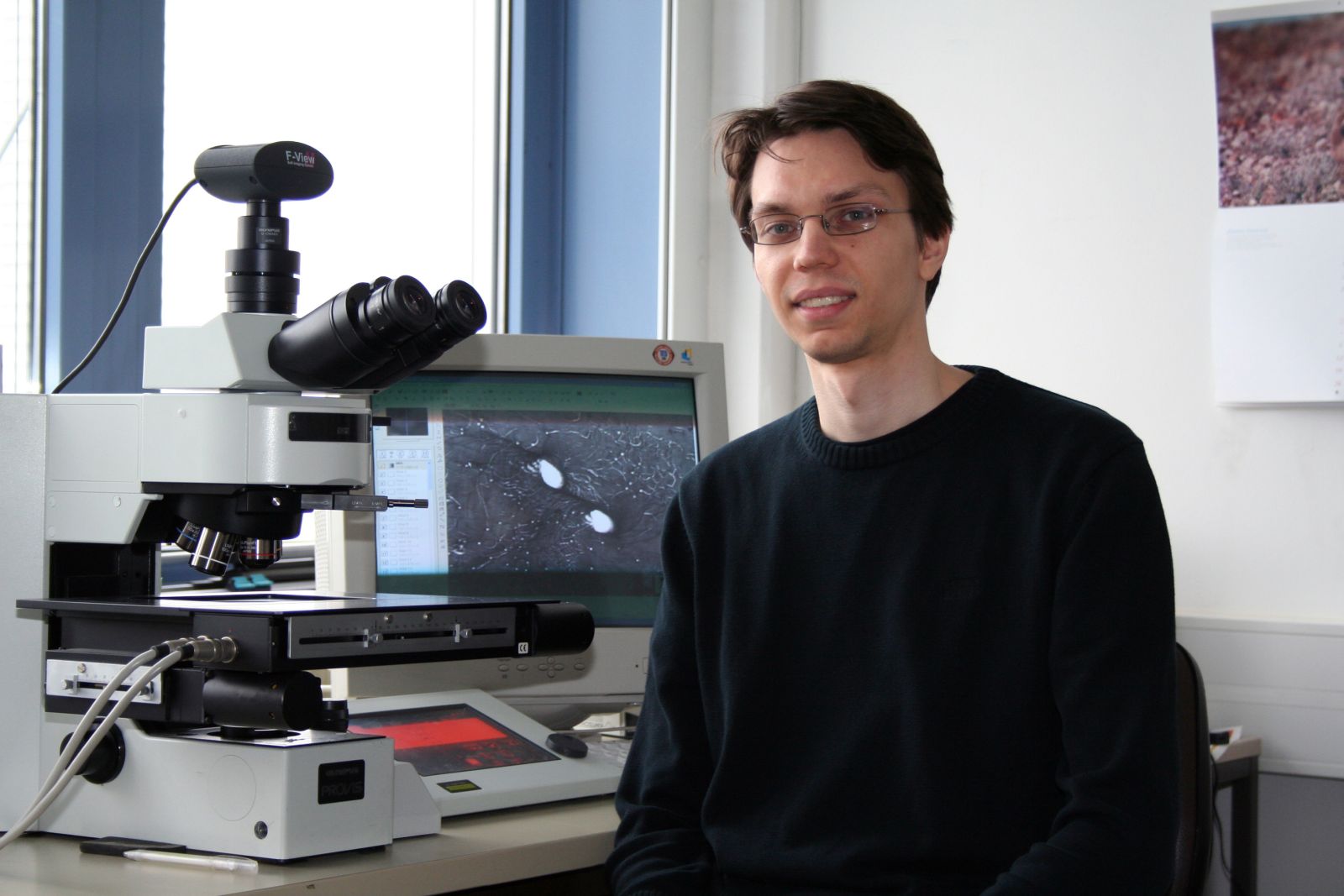
In his thesis project, „Structural defect characterization of 4H-SiC substrates and epitaxial layers using x-ray topography and x-ray diffractometry," Sebastian Polster of the Fraunhofer Institute for Integrated Systems and Device Technology IISB studied these dislocations. He compared the type and number of these crystalline defects using x-ray images that he recorded with the ANKA synchrotron source, with images that were prepared using the conventional etching technique in the laboratory. In this manner, he succeeded in depicting the limits of the established characterization method. The results of this method can now be interpreted with certainty. This is an important basis in order to improve the material regarding the avoidance of critical dislocation types in the material, so that electron devices based on SiC can dominate their market. In recognition of his accomplishments, Sebastian Polster is awarded the 2nd Hugo Geiger Prize.
Growing through holes
An important objective of solar cell research is to produce photovoltaic modules inexpensively, in order to make the power it produces competitive with conventional energy resources. One potential concept to achieve this is the use of crystalline thin-film solar cells, which come from a very thin layer of the expensive, ultrapure silicon. Another option can be found in solar cells whose current-collecting contacts are situated only on the back side of the solar cells, laden with via holes.. Physicist Nils Brinkmann of the Fraunhofer Institute for Solar Energy Systems ISE showed in his thesis project, „Epitaxy through holes: Process development and characterization," how the advantages of both varieties can be brought together.
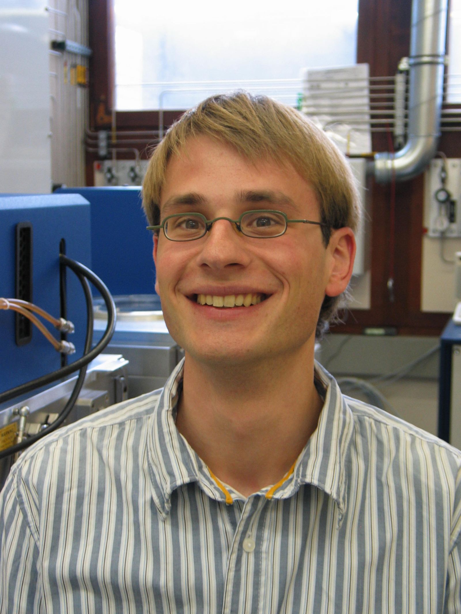
One decisive factor in the new cell concept: minute via holes. The epitaxial layers grow through these on both sides of the thin silicon substrate. This completely new approach was developed by Nils Brinkmann with the aid of Simulations that he then applied in a production process. In addition, he showed how the degree of efficiency of the new solar cells can be further optimized. Nils Brinkmann is awarded the 3rd Hugo Geiger Prize.

