From payment transfers to smart electric meters — for all of these convenient, electronically readable processes, it is crucial to ensure that the products involved cannot be manipulated. Encrypted identifiers or operating protocols in the electronic circuits make sure that is the case. Increasingly, however, there is a challenge in that these security elements can be circumvented. Conventional solutions such as hardware security modules (HSMs) and databases can only provide relative security — plus, they are costly. Dr. Maximilian Lederer from Fraunhofer IPMS and his team have succeeded in identifying a potential solution that is promising in several respects.
Crystallization for multidimensional camouflage
The project being conducted by the experts at Fraunhofer IPMS is based on an effect they first observed in 2020: They discovered that hafnium oxide can crystallize when an alternating electric field is applied. This gives the material ferroelectric properties, meaning that it can generate a spontaneous electrical polarization and shift back and forth between memory states like a light switch.
Based on this discovery, the Fraunhofer researchers are designing components that can change their ferroelectric behavior on a targeted basis through this process, known as electric field-induced crystallization. Since the ferroelectric polarization cannot be read externally, this method unlocks possibilities for elevated security: “We’re creating a system for multidimensional encryption of hardware by storing three properties in our electric field-induced crystallization components: the degree of crystallization, the amount of polarization — by which I mean the ferroelectric phase that is present and the degree to which it is programmed in — and third, the sign for that phase. This can also be visualized in various parameters, such as permittivity and charge,” explains Lederer, the project manager.
Securely in manufacturers’ hands
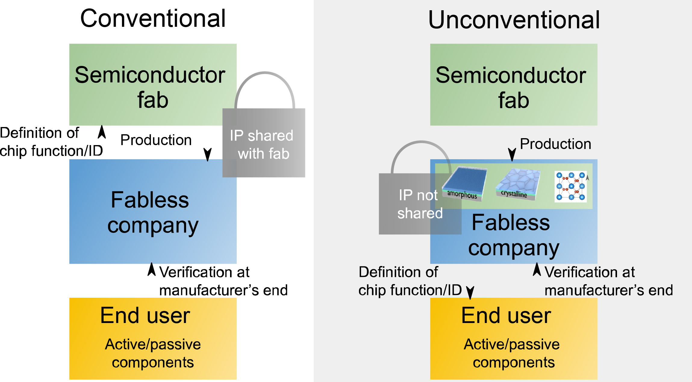
Manufacturers of semiconductors that do not have their own production facilities typically send their system circuit design to external contract manufacturers, share their intellectual property (IP), and then receive the finished component back in the end. This method, however, has some key disadvantages: The functioning of a circuit can no longer be changed, and security features are either hardwired or software-based, which makes it difficult to detect manipulation or counterfeiting. These solutions are also very expensive, and they can only be used in small series. The electric field-induced crystallization process is different.
“With our solution, the functions and properties of the integrated circuit are defined by the company providing the idea, transferred to fabrication, and manufactured there with the electric field-induced crystallization component without there being any need to share the IP behind it. Semiconductor producers can configure a circuit’s function themselves after it is manufactured, using the electrical signals they apply,” Lederer notes. The researchers plan to incorporate their components into advanced microelectronics process flows so that clients that provide ideas can ultimately always decide for themselves what they want their encryption to be like. This is especially interesting for applications in the area of automotive and HSM chips, which are used for bank transfers and other purposes.
The Fraunhofer IPMS specialists firmly believe the new approach will pave the way for mass production of integrated security features. In addition, electric field-induced crystallization circuits are lower in cost and deliver better performance while using less electricity than their standard programmable integrated counterparts, as low voltage is enough to write the three-dimensional states of these elements.
Reliability and bright prospects
The researchers are currently working to demonstrate that their solution works not only at the lab scale but also in an integrated system. Their results so far have been impressive, and potential obstacles have been overcome with flying colors. For example, Lederer and his team were initially concerned that temperature stability could pose a significant challenge, as the electric field-induced crystallization process is thermally dependent.
“We were able to demonstrate that while the effect does depend on temperature, the reliability of the layer created afterward, or of the component, remains constant even at different temperatures. That means we’re not seeing any temperature-dependent losses,” Lederer says, pleased.
The electric field-induced crystallization technology offers impressive development options for semiconductor solutions that are both highly secure and low in cost, but that is not all. Because the hafnium oxide used in the process is compatible with existing semiconductor manufacturing technologies, the researchers also believe there is great potential for rapid transfer to industrial application.
